Driver for the MCP48x2 family of DAC chips from Microchip. More...
Files | |
| file | atmega_spi.c |
| Driver for SPI communication between the ATmega328P and other SPI compatible devices. | |
| file | atmega_spi.h |
| Driver for SPI communication between the ATmega328P and other SPI compatible devices. | |
| file | log_system.c |
| Driver file providing logging functionality over USART, to print debug messages and values to a teminal program on your PC. | |
| file | log_system.h |
| Driver file providing logging functionality over USART, to print debug messages and values to a teminal program on your PC. | |
| file | main.c |
| Example main routine demonstrating the mcp48x2 DAC driver. | |
| file | mcp48x2_dac.c |
| Driver for the MCP4812 10 bit DAC (digital to analog converter) chip. | |
| file | mcp48x2_dac.h |
| Driver for the MCP4812 10 bit DAC (digital to analog converter) chip. | |
| file | pin_defines.h |
| Definitions for pin mapping (for mcp4812_dac) | |
| file | usart.c |
| Driver file providing core USART communication between the target MCU and your PC. | |
| file | usart.h |
| Driver file providing core USART communication between the target MCU and your PC. | |
Detailed Description
Driver for the MCP48x2 family of DAC chips from Microchip.
- See also
- The files can be downloaded from the repo at: https://github.com/Jason-Duffy/AVRly/tree/main/content/modules/data-converters/mcp48x2_dac/example
README
Introduction
The MCP48x2 series from Microchip are dual buffered output Digital to Analog converters available in 8 bit, 10 bit and 12 bit resolutions. These devices operate from a single 2.7V to 5.5V supply and an SPI interface, and can be used for sensor calibration, hardware self-testing, op-amp control, programmable voltage reference and more.
This module was tested on an MCP4812 10 bit DAC, but should also work with the other models if configured correctly. The datasheet for all 3 devices can be found here.
The host MCU sends data to the DAC using the SPI (Serial Peripheral Interface) protocol. For a quick guide on SPI communication, take a look at the module here.
Pinout

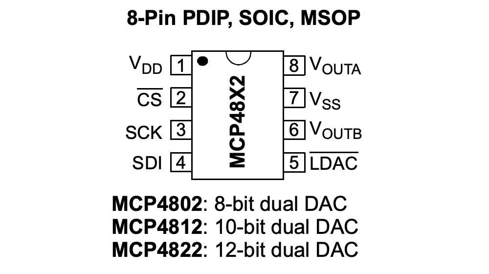
| Pin | Function |
|---|---|
| (1) VDD | Positive supply pin, 2.7V to 5.5V |
| (2) CS | Chip Select pin, device is selected when this is pulled low |
| (3) SCK | Serial Clock signal from host MCU |
| (4) SDI | Serial Data Input pin - same as MOSI |
| (5) LDAC | Latch pin, to control when outputs are updated with new values. Pull low to latch new values into outputs |
| (6) VoutB | Output pin for Channel B |
| (7) Vss | Ground connection |
| (8) VoutA | Output pin for Channel A |
Hookup

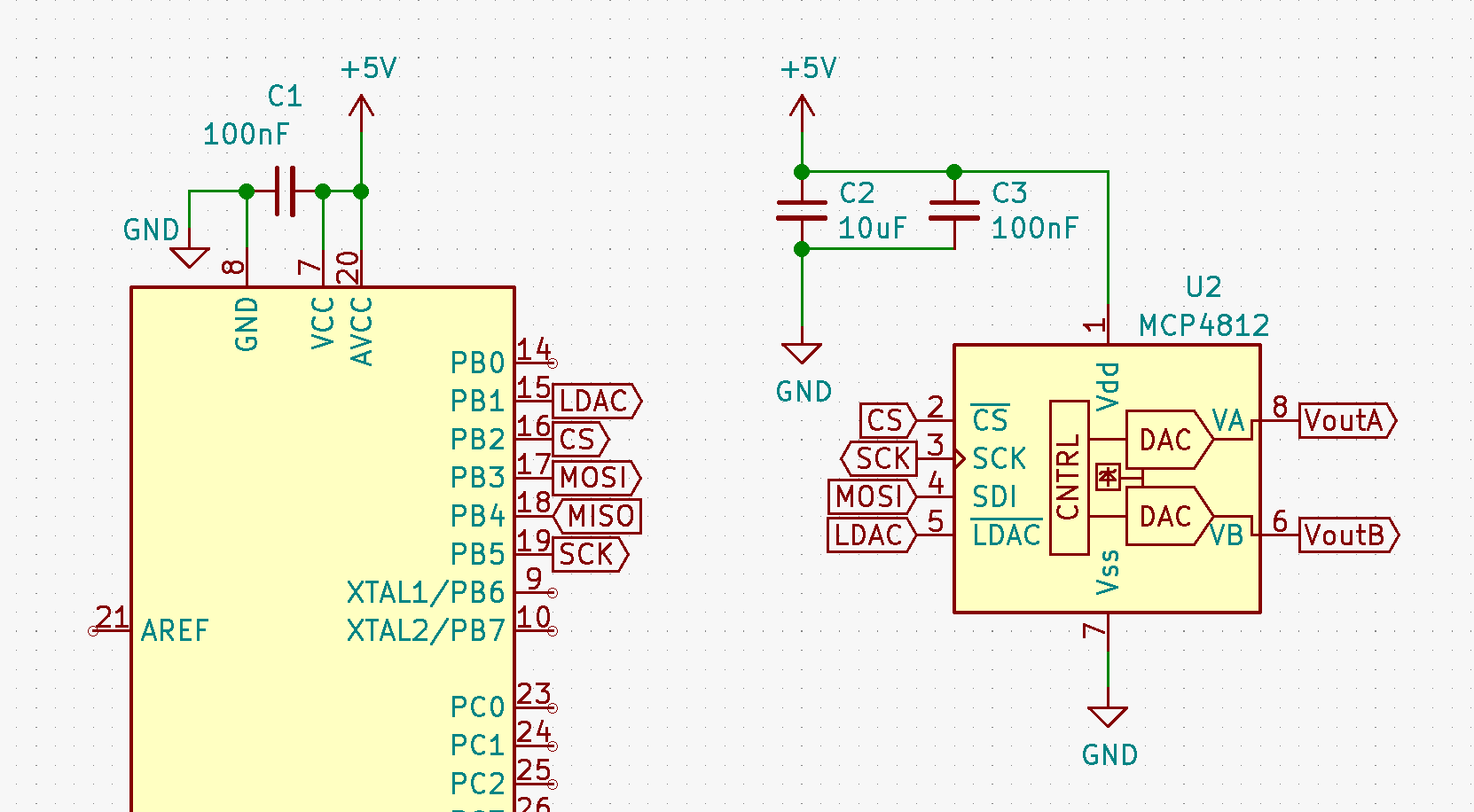
| Pin | Connection |
|---|---|
| (1) VDD | +5V Supply. Decoupling caps are recommended but optional |
| (2) CS | Connect to PB2 |
| (3) SCK | Connect to PB5 |
| (4) SDI | Connect to PB3 |
| (5) LDAC | Optional, if latching of output is desired, connect to PB1. If not required, tie to GND |
| (6) VoutB | Multimeter 1 test probe |
| (7) Vss | Ground |
| (8) VoutA | Multimeter 2 test probe |
Note that there is no connection to the host MCU MISO pin, as this device is write only - the data only goes in one direction, from the MCU to the DAC. The LDAC connection is optional, but is required in this example project. An internal pullup is applied to the MISO pin to ensure it always reads high for the SPI byte trade.
If you connect the output pins to a multimeter (keeping several meters is helpful for tasks like this), you can monitor the output voltage of each channel.
API Reference
Before initialising the DAC for use, you'll need to instantiate a dac_config_t object, and set the configuration values you'd like.
Then pass the address of the config object into the initialisation routine.
Members
| dac_config_t member | Valid Selections |
|---|---|
| model | mcp4802, mcp4812 or mcp4822 |
| sync_manually | true = manual sync, false = sync automatically |
| channel_a.gain_low | true = Gain of 1, false = gain of 2 |
| channel_a.active | true = Channel is active, false = channel is shut down |
| channel_a.level | 0 - 255 for 8 bit DAC, 0 - 1023 for 10 bit DAC, 0 - 4095 for 12 bit DAC |
| channel_b.gain_low | true = Gain of 1, false = gain of 2 |
| channel_b.active | true = Channel is active, false = channel is shut down |
| channel_b.level | 0 - 255 for 8 bit DAC, 0 - 1023 for 10 bit DAC, 0 - 4095 for 12 bit DAC |
When sync_manually is set to true, new voltage levels will not be latched into the output registers until the pulse_latch() function is called. Using this method, you can ensure the voltage level of both channels is updated exactly when required. When sync_manually is set to false, the pulse_latch() function is called automatically when the voltage values are updated.
Unless you need to guarantee a specific voltage output on startup, level can be set to 0.
Setting the Output Voltage
The internal reference voltage (VREF) is 2.048V. When gain_low is set to true, the output range for that channel is from 0.0V to (1023/1024 * 2.048V), roughly a gain of 1. When gain_low is set to false, the output range for that channel is doubled, from 0.0V to (1023/1024 * 4.096V), or roughly 2(VREF).
The resolution of the DAC dictates the increments it can be adjusted to. The MCP4802 has an 8 bit resolution, so the increments can be calculated as 2048mV/(28) = 8mV, or 16mV when gain_low is set to false. For the MCP4812 it's 2mV or 4mV, and for the MCP4822 it's 500µV or 1mV.
So to recap, if we want to set an output voltage of 4092mV, you'd have to set gain_low to false and level to 1023.
Once the DAC is initialised, the output voltage can be set for each channel can be set using the function dac_set_voltage().
The unit here is millivolts, unlike the dac_config_t member variable level which must be calculated based on the resolution of the DAC.
Reconfiguring the DAC
If after initialisation you'd like to change the settings of the DAC, you can change the values of the dac_config_t member variables, then call dac_reconfigure() to update the DAC with those new config settings.